Difference between revisions of "Photovoltaic Effect"
| Line 87: | Line 87: | ||
In other words, charged carriers that have already crossed the junction set up an electric force (field) that acts as a barrier opposing the further flow of free carriers. As more carriers cross the junction, the barrier enlarges, making it increasingly difficult for other carriers to cross. Eventually, an equilibrium is established where (statistically speaking) no more electrons or holes switch sides. | In other words, charged carriers that have already crossed the junction set up an electric force (field) that acts as a barrier opposing the further flow of free carriers. As more carriers cross the junction, the barrier enlarges, making it increasingly difficult for other carriers to cross. Eventually, an equilibrium is established where (statistically speaking) no more electrons or holes switch sides. | ||
| − | |||
| − | + | Since no free charge carriers can rest in a position where there is a potential barrier, the regions on either sides of the junction now become completely depleted of any more free carriers in comparison to the N and P type materials further away from the junction. This zone around the '''PN Junction''' is now called the '''Depletion''' Layer. | |
. | . | ||
| Line 119: | Line 118: | ||
| − | |||
If we then connect the n-type side to the p-type side of the cell by means of an external electric circuit, current flows through the circuit (which responds just as if powered by a battery} because this reduces the light induced charge imbalance in the cell. | If we then connect the n-type side to the p-type side of the cell by means of an external electric circuit, current flows through the circuit (which responds just as if powered by a battery} because this reduces the light induced charge imbalance in the cell. | ||
| − | |||
| − | |||
Negative charges flow out of the electrode on the n-type side, through a load (such as a light bulb}, and perform useful work on that load (such as heating the light bulb's filament to incandescence}. The electrons then flow into the p-type side, where they recombine with holes near the electrode.[[File:PV cell in circuit.png|left|thumb|350x350px]] | Negative charges flow out of the electrode on the n-type side, through a load (such as a light bulb}, and perform useful work on that load (such as heating the light bulb's filament to incandescence}. The electrons then flow into the p-type side, where they recombine with holes near the electrode.[[File:PV cell in circuit.png|left|thumb|350x350px]] | ||
Revision as of 06:39, 22 February 2021
The Sun[edit | edit source]
The sun is the star at the center of the solar system, it has been shinning for more than 4-billion years. It is a nearly perfect sphere of hot plasma with internal convective motion that generates a magnetic field via a dynamo process.
Some stars are enormous sources of X-rays; others mostly generate radio signals. The sun, while producing these and other energies, releases 95% of its output energy as light, some of which cannot be seen by the human eye.
The sun is responsible for nearly all of the energy available on earth. The exceptions are attributable to moon tides, radioactive material, and the earth's residual internal heat. Everything else is a converted form of the sun's energy: Hydropower is made possible due to solar radiant heat; the winds are caused by the sun's uneven heating of the earth's atmosphere; fossil fuels are remnants of organic life previously nourished by the sun; and photovoltaic electricity is produced directly from sunlight by converting the energy in sunlight into free charged particles within certain kinds of materials.
How much Sunlight do we receive on earth?[edit | edit source]
The sun releases a huge quantity of energy in terms of human capacity or need. Power output per second is 3.86 x 10²⁰ megawatts (MW), several billion times the electric capacity of U.S. utilities. This energy is estimated to a near constant supply of 1.37 kilowatts per square meter (kW/m2) here on earth.
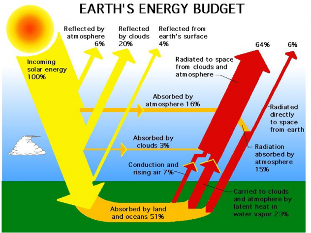
Not all of the direct sunlight incident on earth's atmosphere arrives at the earth's surface as shown below.
The atmosphere attenuates many parts of the spectrum. For example, X-rays are almost totally absorbed before reaching the ground. A good percentage of ultraviolet radiation is also filtered out by the atmosphere. Some radiation is reflected back into space. Some is randomly scattered by the atmosphere, which makes the sky look blue.
It is valuable to relate the amount of sunlight at the earth's surface to the quantity, or air mass (AM), of atmosphere through which the light must pass. The atmosphere is a powerful absorber and can cut the sun's energy reaching the earth by 50% and more. The peak intensity of sunlight at the surface of the earth is about 1 kW/m2. However, not all areas of the earth get the same average amounts of sunshine throughout the year.
How then do we convert this enormous energy into electricity? It all started with a phenomenon called the photovoltaic effect.
Photovoltaic Effect[edit | edit source]
A 19-year-old French experimental physicist named Edmund Becquerel, discovered that when he exposed certain materials to sunlight, he could generate a weak electrical current. This happened in 1839, while he was experimenting with an electrolytic cell made up of two metal electrodes.
He named this phenomenon the "photovoltaic effect". This has since formed the basic process in which a solar cell converts sunlight into electricity.
Understanding a semiconductor[edit | edit source]
A semiconductor is a material that conducts current, but only partly. The conductivity of a semiconductor is somewhere between that of an insulator, which has almost no conductivity, and a conductor, which has almost full conductivity. Most semiconductors are crystals made of certain materials. E.g., Silicon, germanium, gallium arsenide, etc.
Different types of semiconductor have slightly different properties and lend themselves to different applications in various forms of semiconductor devices.
Some may be applicable for standard signal applications, others for high frequency amplifiers, while other types may be applicable for power applications and harsh environments or others for light emitting applications. All these different applications tend to utilise different types of semiconductor materials.
For PV (photovoltaic) applications, we shall take the silicon cell as a model. Silicon is a widely used, typical cell material; understanding the silicon cell is a good groundwork for understanding any PV cell. We shall start by reviewing some of silicon's basic atomic characteristics.
The Silicon atom[edit | edit source]
The silicon atom has fourteen electrons arranged in such a way that the outer four can be given to, accepted from, or shared with another atom. These 4 outer electrons are called valence electrons, they have the highest energy state.
Generally, atoms feel secure when they have 8 electrons on the outer ring, they tend to seek pairs. Silicon creates bonds with other atoms and ends up with 8 electrons in the outer energy shell. Large numbers of silicon atoms combine through their valence electrons, they bond together to form a crystalline structure as seen above.
You must be wondering; how then do they generate electricity? This basic concept above will lead us to understanding the concept of PN Junction.
P-N Junction[edit | edit source]
The P-N Junction is a boundary or interface between two types of semiconductor materials, p-type and n-type, inside a single crystal of semiconductor. Forming a P-type and N-type semiconductor is explained further below.
N-type semiconductor[edit | edit source]
As previously indicated, silicon has 4 valence electrons in its outer shell, all of which are normally part of bonds in a silicon crystal. Suppose by some means we introduce an impurity into an otherwise pure silicon crystal by substituting for a silicon atom an atom such as phosphorus, or antimony having 5 valence electrons.
This impurity atom would occupy the same position in the crystal as a normal silicon atom, supplying an electron for each of silicon's four bonds. But because the phosphorus/antimony atom has one extra valence electron, there would be one electron with no bond to share (Free electron). This impurity atom's extra electron is relatively free.
This free electron behaves as if it were a permanent member of the crystal's conduction band, always ready to be part of an electric current. Overall, the whole crystal would remain neutral, but the crystal's electrical properties would have been drastically altered. Impurities introduced in this way are called dopants, and dopants that have one extra valence electron (such as phosphorus/antimony introduced into a silicon crystal) are called donors because they donate an electron to the crystal. Such a donor-doped crystal is known as n-type because it has free negative charges.
Altering silicon by introducing a donor dopant is part of the process used to produce the internal potential barrier. But n-type silicon cannot of itself form the barrier; a slightly altered silicon with an opposite electrical property is necessary, this takes us to understanding the concept of P-type silicon
P-type semiconductor[edit | edit source]
The second type of an appropriately altered material can be formed by substituting into the silicon crystal, impurity atoms with one fewer valence electron than silicon. An impurity atom with three valence electrons (such as boron) would sit in the position of the original silicon atom, but one of its bonds with the silicon would be missing an electron, i.e., there would be a hole.
As we saw before, holes can move about almost as freely as conduction band electrons. A three-valence-electron impurity in a silicon crystal is called an acceptor because its holes to accept electrons (normally bonded valence electrons or conduction band electrons) from the rest of the silicon crystal.
An acceptor-doped silicon material is called p-type because of the presence of free positive charges (the moving holes). In a p-type material, positive charges are the so-called majority (charge) carriers because they far outnumber any free electrons that in p-type materials are referred to as minority carriers. In an n-type material, where the doping is reversed, electrons (negative charges) are the majority carriers and holes the minority carriers.
Merging the P-type semiconductor and the N-type semiconductor[edit | edit source]
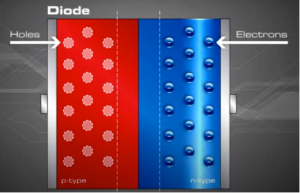
Now that we understand the concept of P and N type semiconductors, the concept of holes and electrons. Let us go one step further to merge the P-type and N-type and understand how electric fields are created.
.
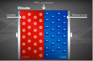
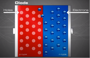
When the n and p materials are in contact, free electrons in the n-type material adjacent to the many holes in the p-type material at the junction will jump into the p-type material, filling the holes. This charge transference process happens rapidly along the dividing line (junction), sending huge numbers of electrons to 'the p-type side and holes to the n-type side.
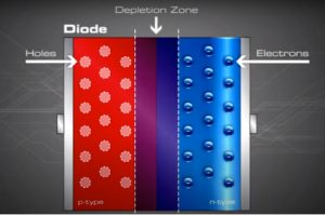
This process continues back and forth until the number of electrons which have crossed the junction have a large enough electrical charge to repel or prevent any more charge carriers from crossing over the junction. Eventually a state of equilibrium will occur producing a “potential barrier” zone around the area of the junction as the donor atoms repel the holes and the acceptor atoms repel the electrons.
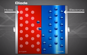
In other words, charged carriers that have already crossed the junction set up an electric force (field) that acts as a barrier opposing the further flow of free carriers. As more carriers cross the junction, the barrier enlarges, making it increasingly difficult for other carriers to cross. Eventually, an equilibrium is established where (statistically speaking) no more electrons or holes switch sides.
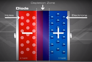
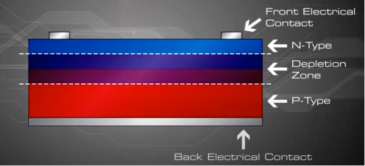
Since no free charge carriers can rest in a position where there is a potential barrier, the regions on either sides of the junction now become completely depleted of any more free carriers in comparison to the N and P type materials further away from the junction. This zone around the PN Junction is now called the Depletion Layer.
.
As the N-type material has lost electrons and the P-type has lost holes, the N-type material has become positive with respect to the P-type which has also turned negative.
Generating current with Photons[edit | edit source]
Now that we understand the concept of depletion layer and the electric field generated, we now represent this basic diode form in the normal way a PV module was created :
How then is the electric current generated ?
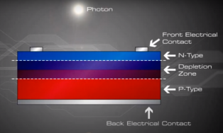
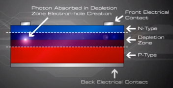
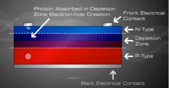
When sunlight or energy from the light (Photons, that has enough energy to free an electron from a bond in the silicon crystal) strikes the PV cell, and is absorbed by the semiconductor in the depletion zone.
.
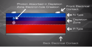
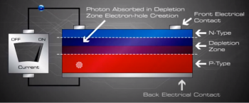
An electron hole pair is created, i.e a free electron and a free hole. Because of the existing electric field at the depletion Zone, this freed electron is attracted to the n-type side, being repelled by the barrier. Likewise, the holes encounter is attracted to the p-type side.
..
Now what? The electrons and holes are free and excited with nowhere to go. The continual incident rays of the photons continue to generate electron hole pairs and charge separation causes the presence of uncombined excess negative charges on the n-type side and excess holes on the p-type side, a charge imbalance exists in the cell.
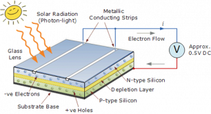
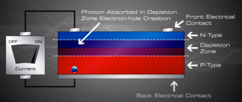
If we then connect the n-type side to the p-type side of the cell by means of an external electric circuit, current flows through the circuit (which responds just as if powered by a battery} because this reduces the light induced charge imbalance in the cell.
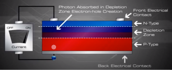
Negative charges flow out of the electrode on the n-type side, through a load (such as a light bulb}, and perform useful work on that load (such as heating the light bulb's filament to incandescence}. The electrons then flow into the p-type side, where they recombine with holes near the electrode.
The light energy originally absorbed by the electrons is used up while the electrons power the external circuit. Thus, an equilibrium is maintained.
The incident light continually creates more electron-hole pairs and, thereby, more charge imbalance; the charge imbalance is relieved by the current, which gives up energy in performing work. The amount of light incident on the cell creates a near proportional amount of current.
And that is the photo-voltaic effect, a work coined from “photo” with the Greek meaning light and “voltaic” meaning voltage.
References & Videos[edit | edit source]
http://www.cs.kumamoto-u.ac.jp/epslab/APSF/Lecture%20Notes/lecture-6.pdf
http://photovoltaicgisashin.blogspot.com/2017/02/the-photovoltaic-effect.html
https://www.nrel.gov/docs/legosti/old/1448.pdf
https://www.electronics-tutorials.ws/diode/diode_1.html
https://www.youtube.com/watch?v=klCwlQhD5Go&feature=youtu.be
https://www.youtube.com/watch?v=ptOgzmC1WkI
